The global laser debonding equipment market is entering a high-growth phase as semiconductor manufacturers increasingly adopt advanced packaging technologies, AI-driven automation, and precision laser processing systems.
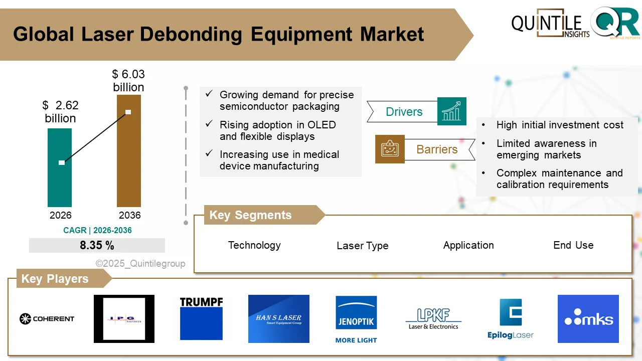
According to recent industry analysis by the market is projected to grow from approximately USD 2.62 billion in 2026 to nearly USD 6.03 billion by 2036, registering a CAGR of 8.35% during the forecast period.
The rapid expansion of fan-out wafer-level packaging (FOWLP), 3D integrated circuits, heterogeneous chip architectures, and chiplet-based semiconductor designs is creating unprecedented demand for high-precision debonding solutions. Laser debonding technology has become increasingly essential in modern semiconductor fabrication because it enables non-contact wafer separation while minimizing material damage and improving manufacturing yield.
As industries worldwide continue moving toward miniaturization, flexible electronics, advanced displays, and energy-efficient devices, laser debonding equipment is evolving into a critical component within the broader semiconductor manufacturing ecosystem.
Request Sample PDF Report: https://www.quintilereports.com/request-sample/1296-laser-debonding-equipment-market/
Advanced Packaging Technologies Fueling Market Growth
One of the primary drivers behind the growth of the laser debonding equipment market is the rising adoption of advanced semiconductor packaging technologies. Semiconductor manufacturers are under growing pressure to improve performance, reduce power consumption, and optimize device compactness.
Technologies such as 3D IC integration, system-in-package (SiP), heterogeneous integration, and FOWLP require highly delicate wafer handling processes. Traditional mechanical separation methods often introduce stress, contamination, and material damage, making laser debonding a more attractive alternative.
Laser debonding systems utilize controlled laser energy to separate temporarily bonded wafers from carrier substrates with exceptional precision. This process minimizes wafer breakage, improves production efficiency, and supports ultra-thin semiconductor manufacturing requirements.
Special Discount: https://www.quintilereports.com/request-discount/1296-laser-debonding-equipment-market/
The shift toward chiplet-based architectures in artificial intelligence processors, high-performance computing systems, and advanced consumer electronics is further accelerating demand for reliable wafer debonding technologies.
AI, Automation, and Smart Manufacturing Reshaping the Industry
Artificial intelligence and industrial automation are significantly transforming the competitive landscape of the laser debonding equipment market. Manufacturers are integrating robotics, AI-powered monitoring systems, and smart factory capabilities into laser debonding solutions to improve throughput, consistency, and operational efficiency.
Advanced automation systems now allow real-time process monitoring, predictive maintenance, adaptive laser calibration, and intelligent defect detection. These innovations help manufacturers reduce downtime, lower operational costs, and achieve superior yield optimization.
AI-driven manufacturing ecosystems are particularly valuable in high-volume semiconductor production environments where microscopic defects can result in major financial losses. By combining laser precision with machine learning analytics, companies are creating highly efficient and scalable production systems.
The growing adoption of Industry 4.0 principles across semiconductor fabrication plants is expected to create long-term growth opportunities for laser debonding equipment providers.
Buying Now: https://www.quintilereports.com/request-enquiry/1296-laser-debonding-equipment-market/
Semiconductor Industry Investments Creating Strong Demand
Global semiconductor investment activity remains one of the strongest contributors to market growth. Governments and private manufacturers are aggressively expanding domestic chip production capacity to address supply chain vulnerabilities and support future technological innovation.
In North America, policy initiatives such as the U.S. CHIPS Act are encouraging large-scale investment in semiconductor fabrication facilities and advanced packaging infrastructure. This trend is driving increased demand for laser processing and wafer handling equipment.
Asia-Pacific continues to dominate global semiconductor manufacturing, with Taiwan, South Korea, China, and Japan making substantial investments in advanced packaging ecosystems. Leading foundries and outsourced semiconductor assembly and test (OSAT) providers are rapidly deploying laser debonding systems to support next-generation chip manufacturing.
Europe is also witnessing rising adoption, particularly in automotive electronics, renewable energy technologies, and industrial automation applications where precision manufacturing is essential.
Medical Devices and Flexible Electronics Expand Application Scope
While semiconductor manufacturing remains the dominant application segment, laser debonding equipment is also gaining traction across medical devices, renewable energy systems, automotive electronics, and flexible display technologies.
Miniaturized medical implants, diagnostic sensors, and wearable healthcare devices require contamination-free and highly accurate assembly processes. Laser debonding technologies help manufacturers separate delicate components without introducing thermal damage or structural defects.
Similarly, the growing popularity of flexible OLED displays, micro-LED technologies, and foldable electronic devices is expanding the commercial scope of precision laser processing solutions.
Battery recycling and renewable energy manufacturing are emerging as additional growth areas. Laser debonding techniques support cleaner material separation processes while reducing waste and improving sustainability in battery recovery operations.
As manufacturers increasingly prioritize environmentally responsible production methods, laser debonding is being recognized as a low-waste and energy-efficient alternative to traditional chemical or mechanical separation technologies.
Ultraviolet and Femtosecond Lasers Driving Technological Innovation
Technological innovation remains central to the evolution of the laser debonding equipment market. Manufacturers are developing advanced laser systems capable of handling increasingly complex materials and packaging architectures.
Ultraviolet (UV) lasers, infrared (IR) lasers, pulsed lasers, fiber lasers, and excimer laser technologies are becoming widely adopted across high-precision manufacturing environments. UV and femtosecond lasers, in particular, are gaining popularity due to their ability to deliver ultra-short pulses with minimal thermal impact.
These technologies provide exceptional control, enabling manufacturers to process delicate substrates while maintaining structural integrity and reducing production defects.
Laser-Induced Forward Transfer (LIFT) technology is also emerging as one of the fastest-growing segments within the market. The process allows highly controlled material transfer during semiconductor packaging and advanced electronics manufacturing.
Additionally, innovations in photothermal and photochemical debonding techniques are expanding the versatility of laser systems across a broader range of industrial applications.
Asia-Pacific Emerging as the Fastest-Growing Regional Market
Asia-Pacific is expected to register the fastest growth rate in the laser debonding equipment market during the forecast period. The region benefits from a strong semiconductor manufacturing base, extensive electronics production infrastructure, and rising government support for domestic chip development.
Countries such as Taiwan and South Korea continue to lead advanced packaging innovation due to the presence of major semiconductor foundries and OSAT providers. China’s ongoing semiconductor self-sufficiency initiatives are also accelerating investment in wafer processing equipment and laser technologies.
Japan remains a critical hub for precision engineering and photonics innovation. Japanese manufacturers are actively developing advanced UV and excimer laser systems tailored for next-generation semiconductor applications.
Meanwhile, North America maintains a strong market position driven by research and development investment, industrial automation adoption, and advanced manufacturing policies.
Europe is steadily expanding its presence through innovation in automotive electronics, renewable energy technologies, and industrial laser engineering.
Competitive Landscape Intensifies Amid Rapid Innovation
The competitive landscape within the laser debonding equipment market is becoming increasingly dynamic as companies focus on automation integration, laser precision enhancement, and smart manufacturing compatibility.
Key market participants include:
- Coherent, Inc.
- IPG Photonics Corporation
- TRUMPF GmbH + Co. KG
- Jenoptik AG
- LPKF Laser & Electronics AG
- MKS Instruments
- Keyence Corporation
Manufacturers are heavily investing in research and development to improve processing speed, reduce thermal impact, and support increasingly complex semiconductor architectures.
Strategic collaborations, acquisitions, and partnerships are becoming common as companies seek to strengthen technological capabilities and expand geographic presence.
Recent developments, including collaborations between Resonac and PulseForge as well as EV Group’s IR LayerRelease solution introduction at SEMICON Korea, demonstrate the market’s strong innovation momentum.
Future Outlook Remains Highly Promising
The future outlook for the laser debonding equipment market remains exceptionally strong as semiconductor complexity, miniaturization, and advanced packaging requirements continue to intensify.
The increasing convergence of artificial intelligence, photonics, industrial automation, and precision manufacturing will likely create new growth opportunities across multiple industries. Manufacturers that successfully integrate AI-driven analytics, sustainable manufacturing processes, and advanced laser technologies are expected to gain a substantial competitive advantage.
As semiconductor fabrication moves toward higher efficiency, lower waste generation, and ultra-thin wafer processing, laser debonding equipment is expected to become indispensable within global electronics manufacturing infrastructure.
The market’s long-term expansion reflects broader technological shifts toward high-performance computing, next-generation displays, renewable energy systems, and intelligent industrial automation.
Frequently Asked Questions (FAQs) for Key Opinion Leaders
1. What is laser debonding equipment used for?
Laser debonding equipment is primarily used to separate temporarily bonded wafers and delicate substrates in semiconductor manufacturing without causing physical damage.
2. Why is laser debonding important in advanced semiconductor packaging?
It enables high-precision, non-contact wafer separation essential for technologies such as FOWLP, 3D IC packaging, and heterogeneous integration.
3. Which industries are driving market demand?
Major industries include semiconductors, electronics, automotive, renewable energy, aerospace, and medical devices.
4. What technologies are commonly used in laser debonding systems?
Key technologies include laser ablation, Laser-Induced Breakdown Spectroscopy (LIBS), Laser-Induced Forward Transfer (LIFT), photothermal debonding, and photochemical debonding.
5. What role does AI play in laser debonding equipment?
AI supports predictive maintenance, real-time monitoring, intelligent calibration, and yield optimization within automated manufacturing environments.
6. Why is Asia-Pacific considered the fastest-growing market?
The region hosts major semiconductor foundries, advanced packaging ecosystems, and government-backed investments in semiconductor self-sufficiency.
7. What challenges does the market face?
High capital costs, technical complexity, workforce training requirements, and competition from alternative debonding methods remain key challenges.
8. How does laser debonding support sustainability goals?
Laser debonding reduces material waste, lowers chemical consumption, minimizes contamination, and improves energy efficiency compared to traditional separation methods.
Our Latest Publication:
Laser Debonding Equipment Market Size, Share & Forecast (2026 – 2036)
Jet Lag Therapy Market Growth 2032: Sleep Tech, Melatonin & Travel Wellness Trends Rising
Adarsh
Business Strategy — Quintile Reports
Adarsh is a Business Strategy professional focused on transforming market insights into actionable growth plans. He supports strategic initiatives through market analysis, competitive intelligence, and data-driven decision-making to help drive long-term business success.
His core skills include strategic planning, market research, growth opportunity assessment, trend analysis, performance tracking, stakeholder communication, cross-functional collaboration, and critical problem-solving.